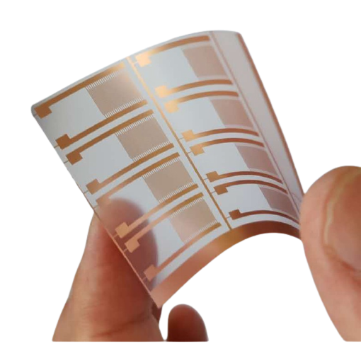
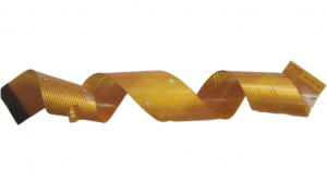
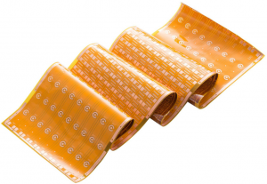
Flexible PCBs are generally classified as follows according to the number of layers and structure of conductors:
1. Single sided FCB:
Single sided flexible PCB has only one layer of conductor, and the surface can have a covering layer or no covering layer.
The insulating base material used varies with the application of the product.
Commonly used insulating materials include polyester, polyimide, polytetrafluoroethylene and soft epoxy glass cloth.
Single sided flexible PCBs can be further divided into the following four categories:
(1)Single sided connection without covering
The wire pattern of this kind of soft PCB is on the insulating substrate, and there is no covering layer on the wire surface.
Like the usual single-sided rigid pcb.
This kind of product is the cheapest one and is usually used in non critical and environmentally friendly applications.
The interconnection is realized by tin welding, fusion welding or pressure welding.It was often used in early telephones.
(2)Covered single-sided connection
Compared with the previous category, this type only has one more layer of covering on the conductor surface according to the customer’s requirements.
When covering, the pad shall be exposed. Simply, it can not be covered in the end area.
If precision is required, clearance hole can be used.
It is the most widely used one of single-sided soft PCB, and is widely used in automotive instruments and electronic instruments.
(3)Double sided connection without covering layer
This kind of connection panel interface can be connected on the front and back of the wire.
For this purpose, a through hole is opened on the insulating substrate at the pad, which can be made by punching, etching or other mechanical methods at the required position of the insulating substrate.
It is used to install elements and devices on both sides and where soldering is required. There is no insulating substrate in the pad area at the path, and this pad area is removed by common chemical methods.
(4)Covered double-sided connection
The difference between this type and the previous type is that there is a covering layer on the surface.However, if the covering layer has access holes, it is also allowed to be terminated on both sides, and the covering layer is still maintained.
This kind of flexible PCB is made of two layers of insulating material and one layer of metal conductor.
It is used in situations where the covering layer needs to be insulated from the surrounding devices, and also needs to be insulated from each other, and the front and back sides of the end need to be connected.
2. Double sided FCB:
Double sided flexible PCB with two layers of conductors.
The application and advantages of this kind of double-sided flexible PCB are the same as those of single-sided flexible PCB. Its main advantage is to increase the wiring density per unit area.
It can be divided into: a no metallization hole and no covering layer;B there is no metallized hole and a covering layer;C. There are metallized holes and no covering layer;D) with metallized holes and covering layer.Double sided flexible PCB without covering layer is rarely used.
3. Multilayer FCB:
Soft multi-layer PCB adopts multi-layer lamination technology like rigid multi-layer PCB, which can be made into multi-layer soft PCB.
The simplest multilayer flexible PCB is a three-layer flexible PCB formed by covering two copper shielding layers on both sides of a single-sided PCB.
This three-layer flexible PCB is equivalent to coaxial conductor or shielded conductor in electrical characteristics.
The most commonly used multi-layer soft PCB structure is a four layer structure, which uses metallized holes to realize interlayer interconnection. The middle two layers are generally power supply layer and grounding layer.
The advantage of multilayer soft PCB is that the substrate film has light weight and excellent electrical properties, such as low dielectric constant.The weight of multilayer flexible PCB made of polyimide film is about 1 / 3 lighter than that of rigid epoxy glass cloth Multilayer PCB, but it loses the excellent flexibility of single-sided and double-sided flexible PCB. Most of these products do not require flexibility.
4. FPC electroplating:
(1) The copper conductor surface exposed after FPC coating process may be polluted by adhesive or ink, as well as oxidation and discoloration caused by high-temperature process. In order to obtain a tight coating with good adhesion, the pollution and oxidation layer on the conductor surface must be removed to make the conductor surface clean.However, some of these pollutants are firmly combined with copper conductors and cannot be completely removed with weak cleaning agents. Therefore, alkaline abrasives with certain strength and polishing brushes are often used for treatment. Most of the adhesives for the covering layer are epoxy resins with poor alkali resistance, which will lead to the decline of bonding strength. Although it will not be obvious, they are not visible in the FPC electroplating process,The plating solution may penetrate from the edge of the covering layer, which will peel off the covering layer in serious cases.During the final welding, the solder is drilled under the covering layer.It can be said that the pretreatment cleaning process will have a significant impact on the basic characteristics of flexible printed board f{c, and the treatment conditions must be paid full attention to.
(2)Thickness of FPC electroplating during electroplating, the deposition speed of electroplated metal is directly related to the electric field strength, and the electric field strength changes with the shape of the line pattern and the position of the electrode. Generally, the thinner the line width of the conductor, the sharper the terminal at the terminal, the closer the distance from the electrode, the greater the electric field strength and the thicker the coating at this part. In the applications related to flexible printed boards, inMany wires in the same line have extremely different widths, which is more likely to produce uneven coating thickness. In order to prevent this, shunt cathode patterns can be attached around the line to absorb the uneven current distributed on the electroplating patterns, so as to ensure the uniform coating thickness on all parts to the greatest extent. Therefore, efforts must be made on the structure of the electrodeA compromise scheme is proposed here. The standards for parts with high requirements for coating thickness uniformity are strict, while the standards for other parts are relatively relaxed, such as lead tin plating for fusion welding and gold plating for metal wire lap (welding), while the requirements for coating thickness are relatively relaxed for lead tin plating for general anti-corrosion.
(3)The stains and dirt of FPC electroplating, the newly electroplated coating state, especially the appearance, did not have any problems, but soon there were stains, dirt, discoloration and other phenomena on some surfaces. In particular, no abnormalities were found during the delivery inspection, but the appearance problems were found when the user received the inspection. This was due to insufficient drifting and residual plating solution on the coating surface,It is caused by slow chemical reaction over a period of time, especially the flexible printed board. Because it is soft and not very flat, its concave is easy to have various solutions”Accumulation” will react and change color at this part. In order to prevent this situation, not only full drifting, but also full drying treatment should be carried out. Whether the drifting is sufficient can be confirmed by high-temperature thermal aging test.
5. FPC electroless plating:
When the circuit conductor to be electroplated is isolated and cannot be used as an electrode, electroless plating can only be carried out. Generally, the plating solution used for electroless plating has strong chemical effect, and the electroless gold plating process is a typical example. The electroless gold plating solution is an alkaline aqueous solution with very high pH. when using this plating process, it is easy to drill the plating solution under the covering layer, especially ifThis problem is more likely to occur because of the lax quality management and low bonding strength of the covering film lamination process.
Due to the characteristics of the plating solution, the electroless plating with displacement reaction is more likely to drill into the overburden. It is difficult to obtain ideal electroplating conditions by this process.
6. FPC HASL:
Hot air leveling was originally developed to coat rigid printed board PCB with lead and tin. Due to its simplicity, it is also applied to flexible printed board FPC. Hot air leveling is to directly and vertically immerse the board in the molten lead and tin bath, and blow away the excess solder with hot air. This condition is very harsh for flexible printed board FPC. If no measures are taken for flexible printed board FPCWhat measures can not be immersed in the solder? The flexible printed board FPC must be clamped between the wire mesh made of titanium steel and then immersed in the molten solder. Of course, the surface of the flexible printed board FPC must be cleaned and coated with flux in advance.
Due to the harsh conditions of the hot air leveling process, it is also easy to drill the solder from the end of the covering layer to below the covering layer, especially when the bonding strength between the covering layer and the copper foil surface is low. Because the polyimide film is easy to absorb moisture, when the hot air leveling process is adopted, the moisture absorbed will cause blistering or even peeling of the covering layer due to rapid heating and evaporation,Therefore, drying treatment and moisture-proof management must be carried out before FPC hot air leveling.