
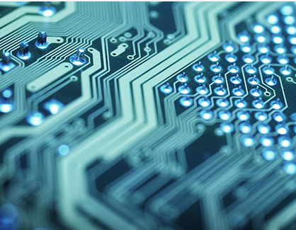
With the continuous improvement of human requirements for living environment, the environmental problems involved in PCB production are particularly prominent. Lead and bromine are the hottest topics. Lead-free and halogen-free will affect the development of PCB in many ways.
Although at present, the change of PCB surface treatment process is not great, as if it is still a distant thing, it should be noted that the long-term slow change will lead to great changes.With the increasing voice of environmental protection, the surface treatment process of PCB will certainly change greatly in the future.
The basic purpose of surface treatment is to ensure good weldability or electrical properties.Since copper in nature tends to exist in the form of oxide in the air, it is unlikely to remain original copper for a long time, so it needs other treatment. Although strong flux can be used to remove most copper oxides in subsequent assembly, strong flux itself is not easy to remove, so it is generally not used in the industry.
There are many PCB surface treatment processes, including hot air leveling, organic coating, electroless nickel plating / gold dipping, silver dipping and tin dipping, which will be introduced one by one below.
1. Hot air leveling (tin spraying)
Hot air leveling, also known as hot air solder leveling (commonly known as tin spraying), is a process of coating molten tin (lead) solder on the surface of PCB and leveling (blowing) with heated compressed air to form a coating layer that not only resists copper oxidation, but also provides good solderability.Hot air leveling solder and copper form copper tin intermetallic compound at the joint.PCB shall sink in molten solder during hot air leveling;The air knife blows the liquid solder before the solder solidifies;The wind knife can minimize the meniscus of solder on the copper surface and prevent solder bridging.
2. Organic solderability protector (OSP)
OSP is a process for surface treatment of copper foil of printed circuit board (PCB), which meets the requirements of RoHS directive.OSP is the abbreviation of organic solderability preserves, which is translated into organic solder film in Chinese, also known as copper protector, and also known as preflux in English.In short, OSP is to grow an organic film on a clean bare copper surface by chemical method.
The film has oxidation resistance, heat shock resistance and moisture resistance to protect the copper surface from further rusting (oxidation or vulcanization, etc.) in the normal environment;However, in the subsequent welding high temperature, the protective film must be easily and quickly removed by the flux, so that the exposed clean copper surface can be immediately combined with the molten solder to form a solid solder joint in a very short time.
3. Full plate nickel gold plating
Plate nickel plating gold is to first coat a layer of nickel on the surface conductor of PCB and then a layer of gold. Nickel plating is mainly to prevent the diffusion between gold and copper.There are two types of nickel gold plating, soft gold plating (pure gold, the gold surface does not look bright) and hard gold plating (the surface is smooth and hard, wear-resistant, contains cobalt and other elements, and the gold surface looks bright).Soft gold is mainly used for making gold wire during chip packaging;Hard metal is mainly used for electrical interconnection at non welded places.
4. Immersion Gold
Gold immersion is to wrap a thick layer of nickel gold alloy with good electrical properties on the copper surface, which can protect PCB for a long time; In addition, it also has the tolerance to the environment that other surface treatment processes do not have. In addition, gold deposition can also prevent the dissolution of copper, which will be beneficial to lead-free assembly.
5. Immersion tin
Since all solders are based on tin, the tin layer can match any type of solder.Tin deposition process can form a flat copper tin intermetallic compound, which makes tin deposition have the same good weldability as hot air leveling without the headache of hot air leveling;Tin sinking plates shall not be stored for too long. They must be assembled according to the sequence of tin sinking.
6. Immersion silver
The silver immersion process is between organic coating and electroless nickel plating / gold deposition, and the process is relatively simple and fast;Even if exposed to heat, humidity and pollution, silver can still maintain good weldability, but it will lose luster.Silver precipitation does not have the good physical strength of electroless nickel plating / gold precipitation, because there is no nickel under the silver layer.
7. Chemical nickel palladium
Compared with gold precipitation, chemical nickel palladium has an additional layer of palladium between nickel and gold. Palladium can prevent corrosion caused by replacement reaction and make full preparations for gold precipitation.Gold is tightly covered with palladium to provide a good contact surface.
8. Hard gold plating
In order to improve the wear resistance of the product and increase the number of plugging, hard gold is plated.
With the higher requirements of users, stricter environmental requirements, and more and more surface treatment processes, it seems a little confusing to choose the surface treatment process with development prospects and stronger universality.The future direction of PCB surface treatment process can not be accurately predicted now. In any case, meeting user requirements and protecting the environment must be done first.

 Jul. 23, 2020


