
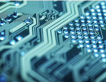
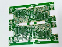
There are many kinds of PCB surface treatment technology. PCB proofing personnel should choose according to the performance and requirements of the board. The following is a brief analysis of the disadvantages of various PCB surface treatment for reference.
1. HASL /Hot air leveling ( tin spraying)
Tin spraying is a common treatment in the early stage of PCB. Now it is divided into lead tin spraying and lead-free tin spraying.
Advantages of HASL
–>Longer storage time
–>After the PCB is completed, the copper surface is completely wetted (completely covered with tin before welding)
–>Suitable for lead-free welding
–>Mature process
–>Low cost
–>Suitable for visual inspection and electrical measurement
Disadvantages of HASL
–>Not suitable for wire binding; Due to the problem of surface flatness, there are also limitations on SMT; Not suitable for contact switch design.
–>Copper dissolves when tin is sprayed, and the board is subjected to a high temperature.
–>For particularly thick or thin plates, tin spraying is limited and the production operation is inconvenient.
2. OSP (organic protective film)
Advantages of OSP
–>The process is simple and the surface is very flat. It is suitable for lead-free welding and SMT.
–>Easy rework, convenient production and operation, suitable for horizontal line operation.
–>The board is suitable for the coexistence of multiple processes (e.g. OSP + ENIG)
–>Low cost and environment-friendly.
OSP disadvantages
–>Limit on the number of reflow soldering (if the film is thick after multiple soldering, it will be damaged. Basically, there is no problem with twice)
–>Not suitable for crimping technology, wire binding.
–>Visual inspection and electrical inspection are inconvenient.
–>N2 gas protection is required during SMT.
–>SMT rework is not suitable.
–>High requirements for storage conditions.
3. Immersion silver
Immersion silver is a better surface treatment process.
Advantages of immersion silver
–>Simple process, suitable for lead-free welding, SMT.
–>The surface is very flat.
–>Suitable for very fine lines.
–>Low cost
Disadvantages of immersion silver
–>High requirements for storage conditions and easy pollution.
–>The welding strength is prone to problems (micro cavity problem).
–>Electromigration and javanni bite of copper under solder mask are easy to occur.
–>Electrical measurement is also a problem
4. Immersion tin
Immersion tin is the most copper tin replacement reaction.
Advantages of immersion tin
–>Suitable for horizontal line production.
–>Suitable for fine line processing, lead-free welding, especially for crimping technology.
–>Very good flatness, suitable for SMT.
Disadvantages of immersion tin
–>Good storage conditions are required, preferably no more than 6 months, to control the growth of tin whiskers.
–>Not suitable for contact switch design
–>The production process has high requirements for the solder resist film, otherwise the solder resist film will fall off.
–>N2 gas protection is preferred for multiple welding.
–>Electrical measurement is also a problem.
5. Electroless nickel/Immersion gold (ENIG)
Nickel gold is a widely used surface treatment process. The nickel layer is a nickel phosphorus alloy layer. It is divided into high phosphorus nickel and medium phosphorus nickel according to the phosphorus content. The application is different. The difference is not introduced here.
Advantages of ENIG
–>Suitable for lead-free welding.
–>The surface is very flat and suitable for SMT.
–>Through holes can also be coated with nickel gold.
–>Longer storage time and less harsh storage conditions.
–>Suitable for electrical testing.
–>Suitable for switch contact design.
–>Suitable for aluminum wire binding, suitable for thick plate, strong resistance to environmental attacks.
6. Electroless Ni/Au (ENEG)
ENEG is divided into “hard gold” and “soft gold”. Hard gold (such as gold cobalt alloy) is often used on gold fingers (contact connection design), and soft gold is pure gold. ENEG is widely used on IC carrier plates (such as PBGA), which are mainly applicable to the binding of gold wire and copper wire. However, the electroplating of IC carrier plate is suitable. The binding gold finger area needs additional conducting wires to be electroplated.
Advantages of ENEG
–>Longer storage time > 12 months.
–>Suitable for contact switch design and gold wire binding.
–>Suitable for electrical testing
Disadvantages of ENEG
–>Higher cost, thicker gold.
–>Plating gold fingers requires additional design wire conductivity.
–>Because the gold thickness is not always, when applied in welding, the solder joint embrittlement may be caused by too thick gold, affecting the strength.
–>Electroplating surface uniformity.
–>The electroplated nickel gold does not cover the edge of the wire.
–>Not suitable for aluminum wire binding.
7. Nickel palladium (ENEPIG)
Nickel palladium is now gradually applied in the field of PCB. Before, it was more applied in semiconductors.Suitable for gold and aluminum wire binding.
Advantages of ENEPIG
–>Applied on IC carrier board, suitable for gold wire binding and aluminum wire binding.Suitable for lead-free welding.
–>Compared with ENIG, there is no nickel corrosion (black disk) problem;The cost is cheaper than ENIG and ENEG.
–>Long storage time.
–>It is suitable for a variety of surface treatment processes and exists on the board.
Disadvantages of ENEPIG
–>The process is complex. Difficult to control.
–>The application history in PCB field is short.


 Jul. 23, 2020


